
Free Semiconductor - explain depletion layer- Question Animation
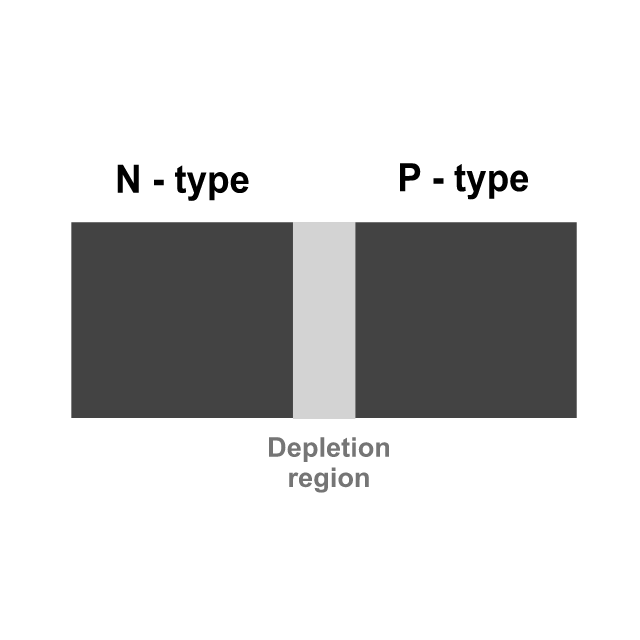
Semiconductor - explain depletion layer A p-n junction diode is a piece of semiconductor material where one side is doped to be p-type and the other side is doped to be n-type. In this set-up, a region will form a both sides of the junction known as the **depletion layer**. What is the depletion layer?
Semiconductor - explain depletion layer A p-n junction diode is a piece of semiconductor material where one side is doped to be p-type and the other side is doped to be n-type. In this set-up, a region will form a both sides of the junction known as the **depletion layer**. What is the depletion layer?
- Optimized dotLottieRecommended
Smallest file size with themes and interactivity.
- dotLottie6.9 KB
Compressed, supports theming and states.
- Optimized Lottie JSON31.7 KB
Optimized JSON for faster loading.
21% smaller than Lottie JSON - Lottie JSON40.1 KB
Standard Lottie format, broad compatibility.
Other export formats
Interactions & plugins
View all


Free to use under the Lottie Simple License